
Executive summary
The last decade has seen extraordinary advances in printed circuit board design and fabrication. There has been substantial advances across design, from schematic entry to simulation to layout and routing to team collaboration and even to the way that manufacturing data is transferred to the fabricator. But there is one place where advancement has seemingly been stalled: the overarching system level hardware architecture design and connectivity.
Introduction
The last decade has seen extraordinary advances in printed circuit board design and fabrication. There have been substantial advances across design, from schematic entry to simulation to layout and routing to team collaboration and even to the way that manufacturing data is transferred to the fabricator. But there is one place where advancement has seemingly been stalled:
the overarching system level hardware architecture design and connectivity.
Although PCB design tools have evolved to become tightly integrated, sharing common databases across the design, and have introduced automation to eliminate human error, hardware systems design has remained much the same as it has been for over a decade.
Siemens has a solution that brings integration, automation and power to multi-board systems design, as an integral part of the Xpedition® design flow.
First, some basic definitions; there are a number of terms used around systems that can often be misunderstood or misinterpreted. For the sake of clarity, let’s define them as:
1. Element – Individual component or sub-assembly that is designed to be part of a larger collaborating function
2. Sub-system or Board – A single printed circuit board (PCB) comprised of digital, analog and/or mixed signal logic that when connected with other boards deliver a higher level of capability and value
3. System or Multi-board system - Independent functioning electronic-centric system packaged as multiple PCBs; COTS components such as actuators, sensors, etc.; all interconnected with cables and/or connectors that deliver features and capabilities that can operate as a standalone complex unit/product.
4. System of Systems - Integration of interdependent systems that create a new, more complex system
These definitions can be applied to all industry segments; whether it is a missile that includes propulsion, navigation, communication, and other systems; or a platform such as an aircraft or car, industrial or medical equipment. The example on the next page shows a medical imaging scanner, itself a product and a combination of several sub-systems, some multi-board, that communicate to provide the complete product capability.

Systems design today
Systems designers today still largely use desktop drawing programs, spreadsheet editors, and document editors.
Once the system has been fully conceptualized, the systems designer can begin to define a logical view of the system interconnect. At the logical level functions are assigned across multiple PCBs, taking into account hardware constraints such as power, cooling, size, weight and physical location within the product.

Multi-board systems may comprise two boards or up to hundreds of boards, packing a cabinet or rack, with interconnected connectors and/or cables and wiring harnesses.
Since the hardware functionality is now distributed across multiple boards, the system integrator must determine the connections that need to be made between each board, and to external interfaces.
Spreadsheets currently are the most commonly used tool to define and manage this connectivity. As design complexity rises, this information may run into tens of thousands of connections.
Once the functionality of each PCB and the interconnections between them have been defined, the design is handed off to the PCB design group. Unfortunately, the interconnectivity data must be manually re-entered, introducing the potential for error.
Of course, no design is static until the first production unit rolls off the line (and even then, it is usually only static until the first Engineering Change Order (ECO)).
From the time of hardware conceptual design until that production unit heads out the door, there will almost certainly be changes to the design. Some of these changes are trivial from the system level perspective; change a screw size, use a different bypass capacitor manufacturer, etc. But, others critically affect the system design, and in particular, the connections and high-pin count connectors between boards.
For example, a particular board may show thermal issues, so several large BGA chips are distributed among several boards to equalize heat dissipation. While it is a fairly easy task to move these to solve a thermal issue, re-defining the connectors among the affected boards is an enormous task and is ripe for errors since it is substantially a manual operation with a spreadsheet.
Once the connectors are re-defined, the data must be sent to the PCB designers to modify the PCB designs, and of course the data is not integrated with the systems designer’s spreadsheet, meaning more manual re-entry, more chance for errors and more risk of further re-spins to “get it right.”
Of course, the electronics industry is not standing still either. Just as the current tools are being taxed to the point of becoming unviable, the complexity continues to increase.
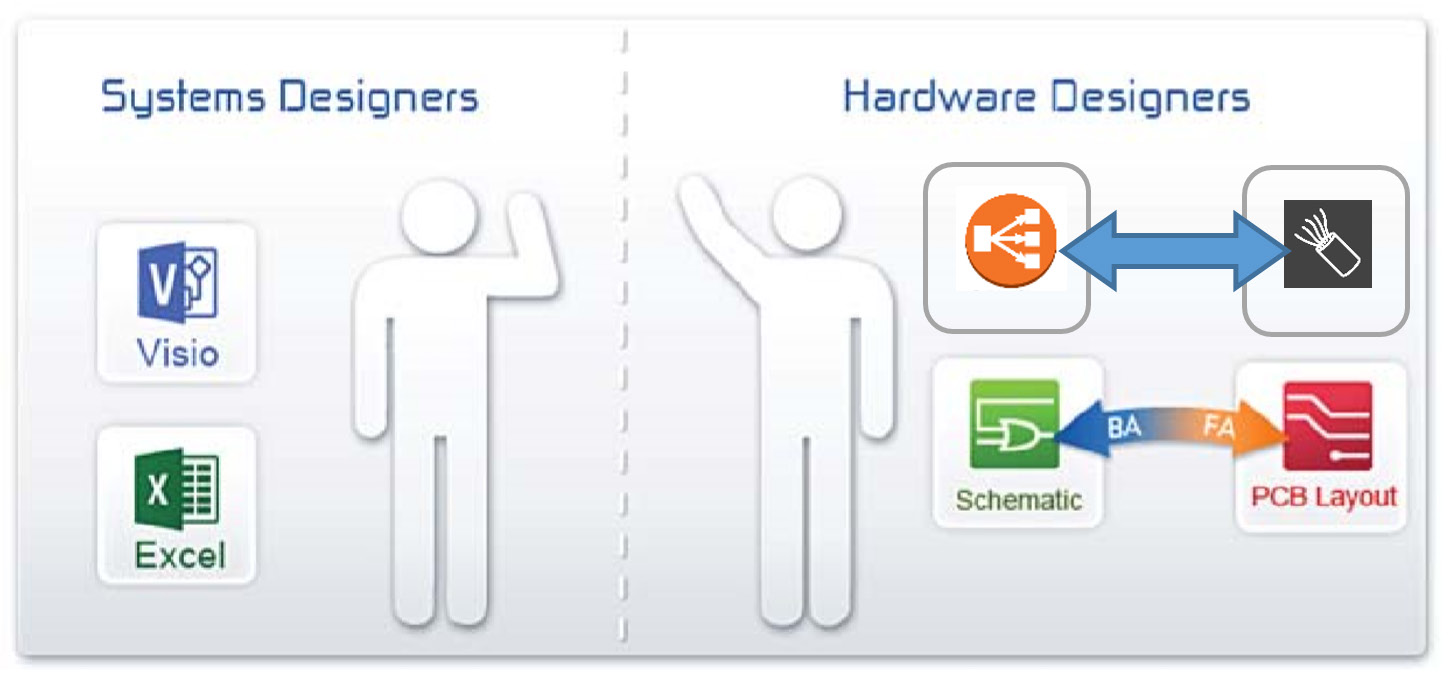
Figure 1: Systems designers typically use MS Visio and MS Excel to define multi-board concept and inter-board connectivity. There is no integration with the hardware designers, who then usually design the system as individual disparate board, cables etc.
Problems with this methodology
The lack of an integrated solution has become the elephant in the room. Everyone sees the problem, but no one has done anything significant about it. Systems design using a drawing tool and a spreadsheet is just not cutting it with the ever expanding complexity and speed of products, coupled with the ever decreasing footprint available for the hardware. The sheer number of hours required to define connector pin assignments and verify connectivity is staggering and even with this level of review, errors get missed, sometimes with devastating financial consequences.
When the inevitable changes occur, each of the affected connectors must be thoroughly checked and rechecked.
This is not just at one level either but at each level where data is manually managed. This means checking at two or more places each time a change is made.
Without an integrated connection between the system design and the PCB design, hours are lost, errors are common and subsequently projects get delayed.
Real-world examples
• A large aerospace manufacturer used the systems design methodology we just described on a very complex system. The system had 1000+ interconnects between the multiple PC boards. One high-power board was designed for right-hand assembly. When in manufacturing, the assembly instructions were mirrored to allow left hand assembly but the connector was not properly translated. The system was destroyed when first powered up and ended up costing the company approximately $7 million in total.
• A smart phone manufacturer found that the power and data connector was too frequently installed upside down; resulting in a relatively inexpensive connector causing a phone to fail inspection and resulting in a substantial rework cost. The solution was to make the connector “ambidextrous” allowing the external connector to be inserted in either orientation. Albeit a clever solution, the resulting circuitry to allow ambidexterity costs the company on each and every phone it manufactures.
What is needed is a systems design tool that enables the user to capture the system design requirements at the logical abstraction level yet be integrated with the PCB design flow. The systems must be bi-directional, allowing forward and backward annotation between the logical view and the physical view to ensure that the entire design system stays in synchronization.
Furthermore, it should accommodate changes and allow partitioning and re-partitioning of functions between PCBs at the logical abstraction level. All interconnections and connectors should be automatically managed, removing manual data entry errors and timeconsuming data re-entry. It should integrate with the PCB design software, sharing PCB contents, constraints, reuse, and variants across the systems design process.
Finally, the environment must be collaborative and concurrent to eliminate bottlenecks.

Figure 2: Connector management can be an enormous problem. Manual methods are open to the introduction of errors.
The Xpedition integrated hardware systems design solution
Xpedition provides a single engineering environment for defining and partitioning electronic systems from the logical system view down to the PCB, reducing the need for interfaces, manual data handling, data duplication and data transfer errors. This means design data is entered once, verified once, and synchronized in a controlled way, eliminating the primary source of errors due to mistakes in basic data entry.
Because of the tight integration across the flow, the data is available to all tools within the flow, including schematic design, PCB layout, and simulation and analysis tools. At no point does any data have to be manually re-entered. Once captured, data is reused throughout the flow.
Logical system-level view enables overall system design optimization through the flow
At the logical system level of the offering design, virtual PCBs can be assigned logical functions based on the partitioning strategy. Here, the systems designer can enter all of the inter- and intra-board connectivity information, instead of using a spreadsheet. This is the only place in the entire flow that this data is entered.
More importantly, this logical abstraction allows design optimization to continue throughout the entire systems design definition cycle. Any time that a function is moved, either locally on the board or to another interconnected board, the connections are automatically updated. There can be no errors introduced by manual data handling.

Figure 3: The scope of the Xpedition product portfolio extends beyond the single PCB to multi-board systems.

Figure 4: Xpedition Systems Designer provides a single engineering environment to capture logical definition of multi-board systems and synchronize logical boards with associated PCB projects.
Connector management
Connector errors can account for a substantial amount of time and money lost on a project. Ongoing “fixes” to eliminate assembly errors can also add a fixed cost to every product. With Xpedition® Systems Designer, these time and monetary costs are eliminated. Not only is interconnect design extremely simple, but automation ensures the proper signals are connected every time. This correct-by-design connector management is an extremely powerful tool, as seen in the example on Figure 6 through Figure 8. Once connections have been made, the connectivity can be quickly verified.

Figure 5: At the logical abstraction level, boards and functions are defined, as are the signal connections between the boards.

Figure 7: Once dragged to the destination, either source or destination connector can be changed to increase or decrease pins by simply dragging and dropping with the cursor.

Figure 6: Connector management is easy - just grab one end and drag it to the destination.

Figure 8: Correct-by-design ensures dynamic signal matching and correctly mated connector pairs... all automatically.
Integrated signal tracing capability
Using signal tracing, users can highlight the entire signal path, reviewing the connections in the report window, as shown in Figure 9. Multiple options allow signals to be traced individually, selectively grouped or by complete connector.

Figure 9: Xpedition provides automation tools to simplify connection verification.
Inter-board cable definition & integration
In many multi-board systems, some or all of the interconnections between boards and other system components (such as sensors) are implemented through point-to-point cabling as well as direct connector coupling. Logical system connectivity can be assigned into multiple cables. Each logical cable requires a physical representation.
Xpedition lets you define, design, and manage the cable design process. Xpedition automates selection of parts by automatically adding wires, multicores, terminals, tapes, and all other cable components to engineer ready-to-manufacture cable designs including bill-ofmaterials and manufacturing drawings. Automatic calculation of quantities (‘true’ manufacturing wire lengths as an example) ensures correct-by-construction cables. Tight integration between ECAD and MCAD environments is essential for an efficient system design process. Mechanical designers can collaborate with cable designers by exchanging critical design decisions that impact on the other side.
External multi-board system connectivty communication
Many multi-board systems have external connectivity, input/output signals, data, power and ground, combinations of both or sometimes even more complex combinations if the multi-board system is part of a much larger system, or system-of-systems. Here there needs to be an efficient, documented, intelligent and manageable process for communicating such logical connectivity to other design teams and/or systems as well as receive such logical connectivity and signal information to ensure external connector selection and signal/pin assignment is made correctly and modified as necessary during revisions. Xpedition communicates external system connectivity (pin/signal assignments, connector descriptions, etc.) using a well-defined data exchange format that is fully supported by the Mentor Capital flow.
Concurrent collaboration
To ensure that no bottlenecks clog the design process, Xpedition provides a collaborative, concurrent design environment including multi-project work-in-progress revision control and management. This environment allows multiple systems designers to work on all system design elements at the same time as multiple hardware engineers are working on the logical and physical PCB designs. As changes are made, they are communicated through the work-in-progress design management hub, ensuring the whole process is kept in sync and nobody is using the wrong revision/version of design IP.

Figure10: Fully integrated design processes for multiple PCBs and associated cables

Figure11: Highly-customizable cable manufacturing drawings
PCB synchronization
Once associations between logical boards and PCB designs are created at the system level, the systems designers can synchronize the content of the logical boards and associated PCB schematics using bi-directional forward and back annotation. System level information passed to the PCB schematic comprises the system connectors and system level blocks. Board designers can push into these blocks and define the underlying logic on the schematic to realize each specific function of the system.
The synchronization process is semi-automatic, requiring execution by the designer; but the software tracks changes between each board and its content, connectivity between the boards and pin-to-pin relationships between connectors. The process provides up-to-date status immediately to all the users involved in the systems design process.
In this way, a change made anywhere within the design stream is propagated forward and backward so that all personnel working on the project have the same up-todate data. Furthermore, this same data is propagated to the Xpedition PCB design flow, ensuring that no manual errors are introduced at what was another manual entry point in the “old” methodology.

Figure 12 The PCB project synchronization cockpit is enabled by forwardand backward annotation throughout the whole design process.
Conclusion
There is a lot of complexity at the hardware system design level. Current methods for managing this complexity have run into limitations in both capacity and process; there isn’t enough time to manually define and manage today’s complex product designs. The result is that the current methods of systems design are taking too long, introduce too many errors from manually handling data, and require redundantly re-entering the same data at multiple points in the design process.
The result of the current methodology has been to insert unnecessary costs, in both time and money, into new product design. Errors cost time, money and lost opportunity. Failure to maintain the integrity of even a single interconnection could result in delay, thousands of dollars to resolve and perhaps even an expensive product recall. To combat these possibilities, some manufacturers have built in “fail safe” precautions, but these too add cost to every unit.
The PCB design realm has seen huge advances in the last decade. What is needed at the multi-board system level is a similar revolution to provide a solution that automates the enormous connection management problem, facilitates easy system and logical design and integrates seamlessly with the PCB design flow while managing team, design and library data at each level of the design hierarchy.
Xpedition’s multi-board systems design capabilities precisely fill that need. It is a single integrated environment that enables multi-board systems design, including logical design, partitioning and connector and wiring management.
Now, your entire hardware design, from multi-board system specification to completed PCBs and cables can be handled with one integrated flow.


工业软件国产替代方案
Sailwind
塔格特Target2000
浩辰Gstar CAD
浩辰Gstar 3D
ZWSOFT中望CAD
ZWSOFT中望3D
Foxit福昕PDF
望友DFx | CAM365

进口正版工业软件
Altium Designer
Valor Process Preparation
Teamcenter Rapid Start
AutoCAD | Inventer
Creo | Windchill
地点:深圳市龙岗区城投商务中心316
联系电话:133 6007 6532
邮箱:sales@yaentek.cn
应用领域
手机通讯
网络机顶盒
汽车电子
新能源
国防军工
工业控制
消费电子